
スマートグラズ向けのQualcomm AR1 Gen1とBestechnic BES2700BPおよびBES2800BPのエンジニアリング比較。ダイサイズ、ISPスループット、NPU TOPS、電力曲線、BOMコストをカバーし、OEMが2025年の正しいプラットフォームを選択を支援します。
投稿日: 8月 03, 2025 - 4,480 ビュー
小米(Xiaomi)やアリババ(Alibaba)がAI搭載スマートグラズの発売を開始するなど、スマートグラズ市場は勢いを増しています。小米のAIグラズはQualcomm AR1とBES2700チップソリューションを採用しており、わずか3日で5万台以上を販売しました。その後,阿里巴巴(Alibaba)も「Wow - Quark AIグラズ」をQualcomm AR1とBES2800構成で発売しました。一方、MetaのRay-Ban Meta AIグラズはQualcomm AR1 Gen1を採用しており、出荷数が200万台を超えています。
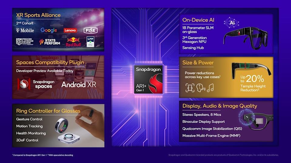
2023年9月に発売されたQualcomm AR1 Gen1は、軽量なAI/ARスマートグラズ向けの specialized processor platformです。6nmプロセス採用により高い集積度と低消費電力を実現し、high-efficiency CPUとGPUを備えたマルチコアアーキテクチャで複雑な計算やリアルタイム画像処理に対応します。第3世代Hexagon NPUは視覚検索やリアルタイム翻訳、指向性音声キャプチャなどの機能をサポートし、最大1280×1280のフルカラー単眼ディスプレイ投影も可能です。
このチップセットにより、IMU、深度カメラ、環境光センサーなどさまざまなセンサー融合が実現し、ユーザーの空間的位置と環境特徴のリアルタイムモニタリングが可能になります。ARアプリケーションの精度とユーザー体験が向上します。写真機能については、第1世代Snapdragon AR1プラットフォームは14ビットデュアルISPを搭載し、最大1200万像素の写真撮影と6メガ像素のビデオ撮影をサポートし、自動露出、自動顔検出、計算HDR、ポートレートモードなどのスマートフォン向け機能も含まれています。
第1世代Snapdragon AR1プラットフォームは拡張性も高く、さまざまな形态のスマートグラズ,支持しています。メーカーはニーズに応じてカスタマイズされた組み合わせと構成を選択でき,例如是否包含3DoF传感器、彩色显示器或更丰富的视觉效果。此外,该平台还配备Qualcomm的FastConnect软件套件,用于XR,支持Wi-Fi 7和Bluetooth 5.2,实现更流畅、更稳定的连接。
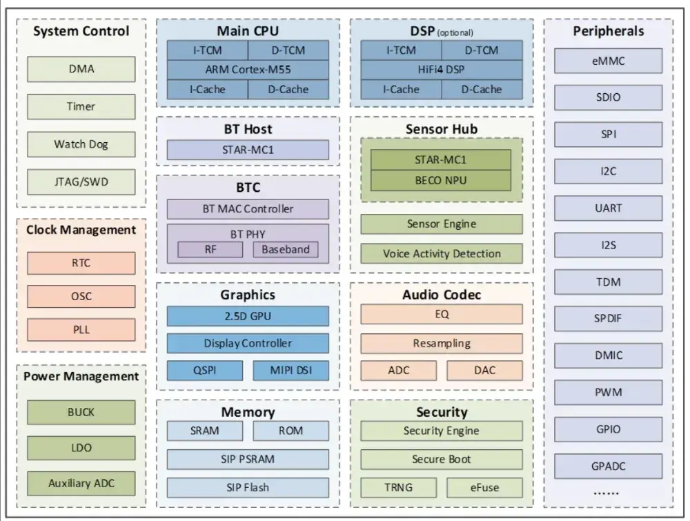
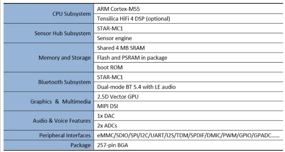
BES Technologies offers three main chips for smart glasses: BES2700BP, BES2800BP, and BES2800HP. The BES2700BP is a low-power, high-performance Bluetooth wearable SoC. It integrates a powerful CPU subsystem, including an Arm Cortex-M55 processor and an optional Tensilica HiFi4DSP, an audio codec subsystem, and a sensor hub subsystem. This combination delivers strong application processing capabilities while significantly reducing power consumption.
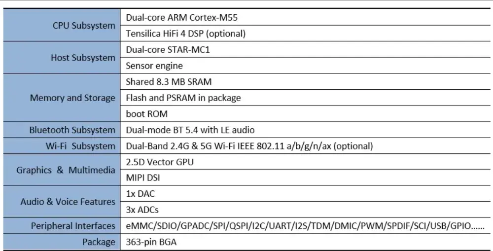
このプラットフォームにはデュアルモード Bluetooth 5.4 サブシステムも搭載されており、クラシック Bluetooth と LE オーディオの両方をサポートしています。さらに、2.5D GPU を備えたマルチメディア サブシステム、最大 4 層のアルファブレンディングをサポートする LCD コントローラー、2 チャンネル DSI を備え、秒間 60 フレームで最大 500x500x32 ビットの解像度をサポートできます。
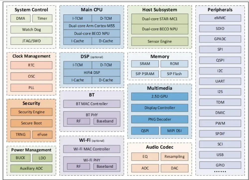
BES2800 は 6nm FinFET プロセスで製造されており、 멀티코어 CPU/GPU、NPU、大容量ストレージ、低消費電力 Wi-Fi、デュアルモード Bluetooth を統合しています。これにより、パフォーマンス、電力効率、技術革新において大幅な改善が実現し、TWS イヤホンやスマートウォッチ、スマートグラズ、補聴器などのウェアラブル機器に堅牢なコンピューティング力と高品質なシームレスな接続を提供します。
BES2800 ベースのスマートグラズ ソリューションは、完全に統合された音声入出力を備え、軽量モデルのローカル動作を可能にします。その低消費電力デュアルモード Wi-Fi/BT により、一部のオンライン音声 AI 要件とクラウド間の迅速な対話が可能になります。主流の ISP チップと連携して、ビデオや写真機能および画像認識を備えたマルチモーダル スマートグラズ システムを形成し、より長い装着時間を実現します。
BES2800 は強力な低消費電力ワイヤレス音声処理システムとして、プロフェッショナルオーディオデバイスが求めるマルチストリーム、高帯域幅、低遅延、長時間音声伝送の要件を満たしています。従来の狭い帯域のBluetoothオーディオ伝送のみをサポートするBluetoothコントローラーとは異なり、BES2800 プラットフォームは低消費電力 Wi-Fi プロトコル伝送を利用して、30 倍以上のデータレートとミリ秒レベルのレイテンシを達成しています。
ウェアラブルにおけるAI演算ニーズの高まりとバッテリーサイズの大幅な増加がない現状を踏まえ、SoCチップは演算力を強化し消費電力を抑える先进工艺の採用が不可欠です。BES は SoC チップの低消費電力条件下での演算性能を高めるため、新世代の NPU と ISP システムを開発しました。新世代 NPU はより低い消費電力でより強力な演算力を提供し、ピーク演算容量は TOPS 到達をサポートします。異なる演算力とモデルシナリオに対応するため MAC 数動的切り替えをサポートし、最適な電力とパフォーマンスの割り当てを実現します。 various lightweight CNN and RNN models supported, facilitating rapid deployment of customized AI algorithms.
компания разработала новую ISP с поддержкой камер до десятков миллионов пикселей, с поддержкой multi-camera fusion technology, dual-exposure HDR technology, and camera motion fusion technology для повышения адаптируемости платформы к смарт-очкам. Additionally, the ISP incorporates camera post-processing characteristics, allowing wearable platforms to quickly process video and image signals at extremely low power levels through hardware-accelerated processing, delivering output to users.
Another bottleneck in local AI computing power operation is efficient memory bandwidth. To address this, the company has developed new-generation low-power LPDDR and MIPI PHY high-speed interface technologies. These significantly optimize the power consumption of AI operation on wearable devices, extending battery life.
BES's wearable platform chips are gradually transitioning to a more advanced 6nm FinFET process, which substantially reduces digital power consumption compared to previous processes. As the market's demand for low-power wireless transmission continues to rise, the company has utilized the fast speed and low power consumption of advanced-process digital circuits. It has developed a new digital-architecture-based Bluetooth transmitter system and commercialized it, with transmission power adaptively adjusting according to performance. In wireless reception, a new-generation receiver has been developed, achieving significantly improved sensitivity and transmission distance under the same power consumption.
According to sources, BES's smart glasses SoC chip project primarily focuses on single-chip integration of low-power display technology, image sensing technology, and orientation acceleration sensor technology. It also aims to upgrade multi-protocol and multi-standard wireless transmission technologies.
The BES2800 employs a system-level SoC solution. Using a 6nm process, it integrates multi-core CPUs/GPUs, NPUs, low-power Wi-Fi, and Bluetooth modules, providing high-performance computing and connectivity for AI glasses. However, to meet the shooting function requirements of AI glasses, it needs to be paired with an external ISP chip.
Currently, AI glasses solutions mainly include single SoC solutions, MCU-level SoC + ISP solutions, and SoC + MCU solutions. These solutions are competing against each other. According to IDC data, global smart glasses shipments are expected to reach 12.05 million units by 2025, representing an 18.3% year-on-year growth. Smart glasses are likely to experience explosive growth driven by major manufacturers and a thriving industrial chain.
